
Filter articles
标签
产品
Loading...

验证汽车零部件的规格
在汽车零部件的开发和生产过程中,无论是供应商还是汽车制造商,都必须符合规格要求。这些规格对保持汽车和其他车辆在生命周期内的性能标准和安全运行至关重要[1,2,3]。在满足或超越日益严格的质量标准的同时,对更高效和更具成本效益的零部件开发和生产的需求一直在提高。本文解释了如何用数码显微镜轻松快速地研究和记录零件以确定其是否符合规格要求。
Loading...
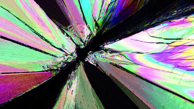
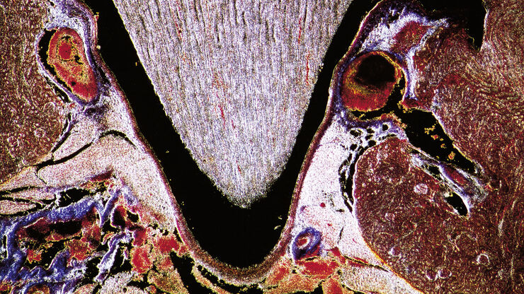
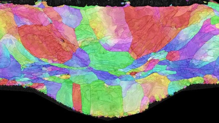
偏振光显微观察
偏光显微镜通常应用于材料科学和地质学领域,根据矿物的折射特性和颜色来识别矿物。在生物学中,偏光显微镜通常用于晶体等双折射结构的识别或成像,或用于植物细胞壁中纤维素和淀粉粒的成像。
Loading...
. With DIC users are able to visualize small height differences on the wafer surface more easily.")
6英寸晶圆检测显微镜:可靠观察细微高度差异
本文介绍了一种配备自动化和可重复的DIC(微分干涉对比)成像的6英寸晶圆检测显微镜,无论用户的技能水平如何。制造集成电路(IC)芯片和半导体组件需要进行晶圆检测,以验证是否存在影响性能的缺陷。这种检测通常使用光学显微镜进行质量控制、故障分析和研发。为了有效地可视化晶圆上结构之间的小高度差异,可以使用DIC。
Loading...
![[Translate to chinese:] Optical microscope image, which is a composition of both brightfield and fluorescence illumination, showing organic contamination on a wafer surface. The inset images in the upper left corner show the brightfield image (above) and fluorescence image (below with dark background).](/fileadmin/_processed_/a/1/csm_Organic_contamination_on_a_wafer_surface_6699165cee.jpg "[Translate to chinese:] Optical microscope image, which is a composition of both brightfield and fluorescence illumination, showing organic contamination on a wafer surface.")
晶圆上的光刻胶残留和有机污染物的可视化
随着半导体上集成电路(IC)的尺寸低于10纳米,在晶圆检测中有效检测光刻胶残留等有机污染物和缺陷变得越来越重要。光学显微镜仍然是常见的检测方法,但对于有机污染物,明场和其他类型的照明可能会存在局限性。本文讨论了荧光显微镜如何在半导体行业的QC、故障分析和研发过程中有效检测晶圆上的光刻胶残留和其他有机污染物。
Loading...

数码显微镜摄像头和图像分析的基础技术术语定义
现今绝大多数显微镜都配置了摄像头。摄像头的特征通常决定了所采集到的图像是否能够揭示出研究人员希望观察到的现象。但深入到摄像头术语时,技术术语十分繁杂。我们汇总整理了最为重要的术语及其简明释意以便提供方向。这些术语按字母顺序排列。
![[Translate to chinese:] Images of the same area of a processed wafer taken with standard (left) and oblique (right) brightfield illumination using a Leica compound microscope. The defect on the wafer surface is clearly more visible with oblique illumination.](/fileadmin/_processed_/9/1/csm_Processed_wafer_standard_and_oblique_brightfield_illumination_556d919235.jpg "[Translate to chinese:] Images of the same area of a processed wafer taken with standard (left) and oblique (right) brightfield illumination using a Leica compound microscope. The defect on the wafer surface is clearly more visible with oblique illuminati")
Loading...
![[Translate to chinese:] Preparation of an IC-chip cross section: grinding and polishing of the chip cross section.](/fileadmin/_processed_/3/b/csm_Grinding_polishing_EM_TXP_81f93bc20c.jpg "[Translate to chinese:] Preparation of an IC-chip cross section: grinding and polishing of the chip cross section.")
电子产品制造截面分析
本文将讨论印刷电路板 (PCB) 和总成 (PCBA)、集成电路 (IC) 和电池组件的横截面为什么对质量控制 (QC)、故障分析 (FA) 和研发 (R&D) 有效,以及如何制备这些横截面。
