
Filter articles
标签
产品
Loading...
![[Translate to chinese:] Optical microscope image, which is a composition of both brightfield and fluorescence illumination, showing organic contamination on a wafer surface. The inset images in the upper left corner show the brightfield image (above) and fluorescence image (below with dark background).](/fileadmin/_processed_/a/1/csm_Organic_contamination_on_a_wafer_surface_6699165cee.jpg "[Translate to chinese:] Optical microscope image, which is a composition of both brightfield and fluorescence illumination, showing organic contamination on a wafer surface.")
晶圆上的光刻胶残留和有机污染物的可视化
随着半导体上集成电路(IC)的尺寸低于10纳米,在晶圆检测中有效检测光刻胶残留等有机污染物和缺陷变得越来越重要。光学显微镜仍然是常见的检测方法,但对于有机污染物,明场和其他类型的照明可能会存在局限性。本文讨论了荧光显微镜如何在半导体行业的QC、故障分析和研发过程中有效检测晶圆上的光刻胶残留和其他有机污染物。
Loading...
![[Translate to chinese:] Image of burrs (red arrows) at the edge of a battery electrode acquired with a DVM6 digital microscope.](/fileadmin/_processed_/7/6/csm_Burrs_at_the_edge_of_a_battery_electrode_b8ae4a8491.jpg "[Translate to chinese:] Image of burrs (red arrows) at the edge of a battery electrode acquired with a DVM6 digital microscope.")
电池制造过程中的毛刺检测
毛刺是电池电极片边缘可能出现的缺陷,例如在制造过程中的分切环节。它们可能会因诸如短路等故障导致电池性能下降,并引发安全和可靠性问题。毛刺检测是电池生产质量控制的重要部分,对于生产具有可靠性能和寿命的电池至关重要。通过适当照明的光学显微镜可以在生产过程的关键步骤中快速可靠地对电极上的毛刺进行视觉检测。
![[Translate to chinese:] Images of the same area of a processed wafer taken with standard (left) and oblique (right) brightfield illumination using a Leica compound microscope. The defect on the wafer surface is clearly more visible with oblique illumination.](/fileadmin/_processed_/9/1/csm_Processed_wafer_standard_and_oblique_brightfield_illumination_556d919235.jpg "[Translate to chinese:] Images of the same area of a processed wafer taken with standard (left) and oblique (right) brightfield illumination using a Leica compound microscope. The defect on the wafer surface is clearly more visible with oblique illuminati")
Loading...

如何提高微电子元件检测性能
在检查硅片或微机电系统时,你需要看更多吗?你想得到与电子显微镜相似的清晰详细的样本图像吗?
观看这个免费的网络研讨会,了解更多关于强大的成像和对比技术,可以提高您的检查性能。您将了解如何克服分辨率标准,而不需要浸油或转移到SEM,以实现您想要的检测结果。
Loading...
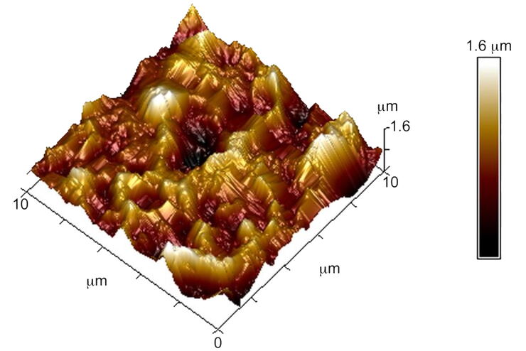
表面计量学简介
本报告简要讨论了几种常用于评估表面形貌(也称为表面纹理或表面光洁度)的重要计量技术和标准定义。随着纳米技术、薄涂层以及电路和装置小型化的出现,表面计量学已成为一个极其重要的科学和工程领域。
